Why this exists
Itron makes infrastructure for utilities — electricity, gas, and water metering, plus the communication networks those meters live on. A utility’s meters run on batteries that have to last fifteen or twenty years in the field, often in environments (junction boxes, underground vaults, the sides of houses in northern Idaho) where replacing them is expensive. The math is brutal: a meter that draws 10 µA average runs out of battery roughly twice as fast as one that draws 5 µA.
Most of a meter’s life is spent asleep. The meter wakes briefly to read a sensor, accumulate a measurement, occasionally transmit data over the utility’s wireless network, then goes back to sleep for seconds, minutes, or hours depending on the application. Sleep current dominates the energy budget. Every µA of quiescent draw is a year of battery life over the deployment lifetime.
The other constraint is that Itron’s meters cover a wide range of sensor types — current transformers, Rogowski coils, water flow sensors, gas pressure transducers, temperature probes — with wildly different signal levels, source impedances, and noise environments. Designing a separate front-end board for each sensor type is the expensive way to do it. The interesting way is to design one front-end that can be configured for many sensor types through gain and filter settings, and run on the same low-power architecture regardless of what it’s measuring.
EN26-59 is that one front-end. The capstone scope: design it, lay it out, get it manufactured, validate it.
The project came to us through Gonzaga’s capstone program, which matches student teams to sponsor-proposed projects based on interest and skill fit. Itron put forward the universal-sensor-board concept; our team picked it because the combination of mixed-signal layout, ultra-low-power design, and an actual manufacturing outcome was the kind of work nobody gets in coursework alone.
What it does
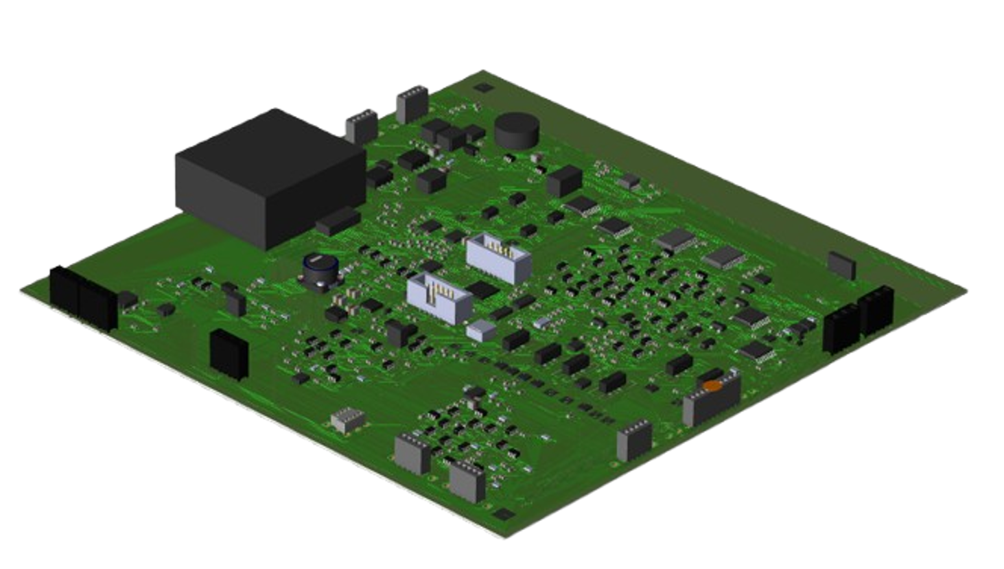
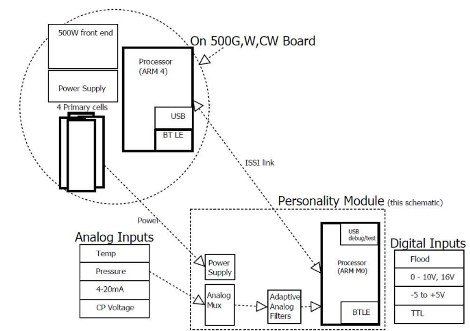
EN26-59 is a roughly business-card-sized 4-layer PCB with four functional blocks:
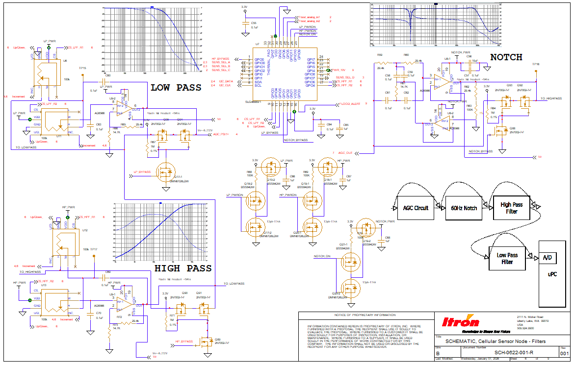
- A configurable analog front-end — single-ended or differential input, 9-step programmable gain, anti-alias filter, ADC sampling into the MCU
- A microcontroller and memory — Apollo3 Blue (Cortex-M4F at ~96 MHz, ultra-low-power architecture, 49-ball BGA at 0.4 mm pitch), with external storage for measurement buffering
- A power management subsystem — Dialog GreenFET load switches gating each subsystem independently, a GreenPAK programmable mixed-signal IC handling wake-on-event logic and power sequencing, voltage regulators sized for the µA budget
- A wireless subsystem — a 2.4 GHz radio path terminating in an inverted-F antenna we designed and tuned on-board, with a controlled-impedance 50 Ω feed and a deliberate ground-plane keep-out under the radiating element
The “universal” in “universal sensor board” refers specifically to the front-end. Through the gain steps and a small number of jumper or solder-strap configuration options, the same board services sensors that produce signals from millivolts up to volts, single-ended or differential, with source impedances from ohms to kilohms.
The architecture decisions that mattered
A 4-month capstone project is short. Most of the real engineering happened in the first six weeks of architecture decisions — once those were locked in, the rest was execution. I want to walk through the three architectural decisions that shaped the rest of the project, because they’re the parts of the work that generalize beyond this specific board.
Decision 1: Apollo3 Blue, BGA, and what that costs
The sub-2 µA quiescent target effectively chose the MCU. Most modern low-power MCUs claim “ultra-low-power” sleep modes, but the actual deep-sleep current with all the realistic gotchas (RAM retention, RTC running, brown-out detector enabled, external sensors quietly leaking through their inputs) often lands in the 5–20 µA range. Apollo3 Blue is one of the few MCUs that genuinely hits the sub-µA mark in deep sleep with RAM retention. It also runs at 6 µA/MHz when active, which means waking, sampling, and going back to sleep is cheap.
The cost of that choice: 49-ball BGA, 0.4 mm pitch. For a student team this is a meaningful escalation. The Apollo3 Blue isn’t available in a QFN package; if you want the part, you take the BGA. That means:
- 4 layers minimum (you cannot fan a 49-ball 0.4mm BGA out on 2 layers, full stop)
- Via-in-pad for the inner rows — there is no other way to escape the central balls of a 7×7 grid at this pitch
- A reflow profile that has to be right the first time — these aren’t being hand-soldered
- Manufacturing tolerances that put us into “small-batch professional fab” territory, not “OSH Park 4-layer”
Michael Baker owned the power-tree topology and the initial BGA pad geometry — defining the via-in-pad pad/aperture dimensions, the rail decoupling network on layer 3, and the supply-routing constraints I had to honor when I did the escape. Working from those constraints, I made the escape strategy split: dogbone fanout for the outer two rows (balls accessible without via-in-pad, escape on layer 1 with short stubs to a normal via), and a diamond via-in-pad pattern for the central 3×3 (the inner balls that have no external clearance). The diamond pattern was the version that survived after I tried a straight-grid via-in-pad fill and ran out of escape channels on layer 4 — staggering the inner vias diagonally opened up the routing channels between them just enough to get every inner signal out. Final minimum trace width on the BGA escape came in at ~3 mil (0.075 mm), which is the floor of what Itron’s PCB partner will run reliably on a 4-layer stackup. Every BGA-adjacent trace was hand-routed; I did not trust the autorouter on geometry this tight.
Apollo3 Blue was the right call, but it’s the decision that turned the project from “a low-power sensor board” into “a low-power sensor board that has to be manufactured properly the first time.” Every other downstream choice flowed from this one.
Decision 2: The LT1996 PGA, and why discrete gain steps
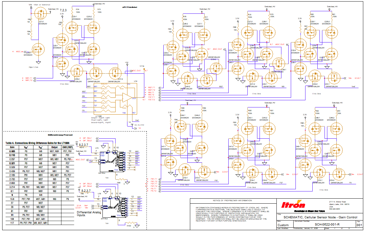
The programmable gain stage is the heart of the universal front-end. The LT1996 is a precision instrumentation amplifier with an unusual feature: it has an internal resistor ladder accessible at external pins, designed to be tapped at different points to give discrete gain settings. We use an analog multiplexer to select among 9 taps, producing 9 gain steps from −19 dB to +38 dB.
There were two natural alternatives, and ruling them out is the more interesting part of the story.
Alternative A: a digitally-programmable continuous-gain amp (an LTC6915, an MCP6S series, or similar). These are convenient — write to a register, get a gain. They’re also noisier than instrumentation amps with passive ladders, have worse common-mode rejection, and consume static current that an LT1996 + mux topology doesn’t. For a sub-2 µA target, the quiescent draw of the convenient option was a non-starter.
Alternative B: an external resistor network with mechanical switches or solder straps. Cheap, low-noise, no static current. The problem: it’s not programmable. The MCU can’t change gain mid-deployment, which kills the dynamic-range advantage of having gain at all — for a sensor that produces a wide range of signal amplitudes, the board can’t compensate without physical intervention. For a universal sensor board, that’s the wrong tradeoff.
The LT1996 + analog mux topology was the third option that took longer to design but won on every relevant axis: low static current, real programmability, excellent noise, accurate gain steps (the internal ladder is laser-trimmed, so the step accuracy is set by silicon, not by external 1% resistors).
Decision 3: GreenPAK as a programmable glue layer
Apollo3 Blue is excellent but it’s not the right thing for every job on the board. A specific example: the wake-on-event logic. Imagine a current sensor with a threshold — the meter should sleep until current exceeds X, then wake the MCU to start measuring. Implementing that with an MCU pin requires the MCU to be awake enough to monitor the pin, which defeats the purpose.
The clean architecture is to have a tiny piece of always-on logic that watches the sensor, decides when something interesting happened, and only then wakes the MCU. That’s a job for either a small discrete-logic circuit, a dedicated comparator IC plus a flip-flop or two, or — the option we picked — a Dialog GreenPAK programmable mixed-signal IC.
A GreenPAK is roughly: a few comparators, a few op-amps, a few flip-flops, a few logic gates, and a small analog crossbar, all in a chip the size of a 1206 resistor, with picoamp standby current, programmed through a one-time-programmable interface. For maybe 30 cents in volume, it replaces a half-dozen discrete parts and lets us reconfigure the wake-on-event behavior in firmware-equivalent terms (you don’t reprogram in the field, but the design itself is flexible up until manufacturing).
The GreenPAK also handles power sequencing. The Apollo3 Blue, the radio subsystem, and the analog front-end each have their own supply rail. They need to come up in the right order at power-on and shut down in the right order at sleep. The GreenFETs (the load switches) provide the actual switching; the GreenPAK provides the sequencing logic.
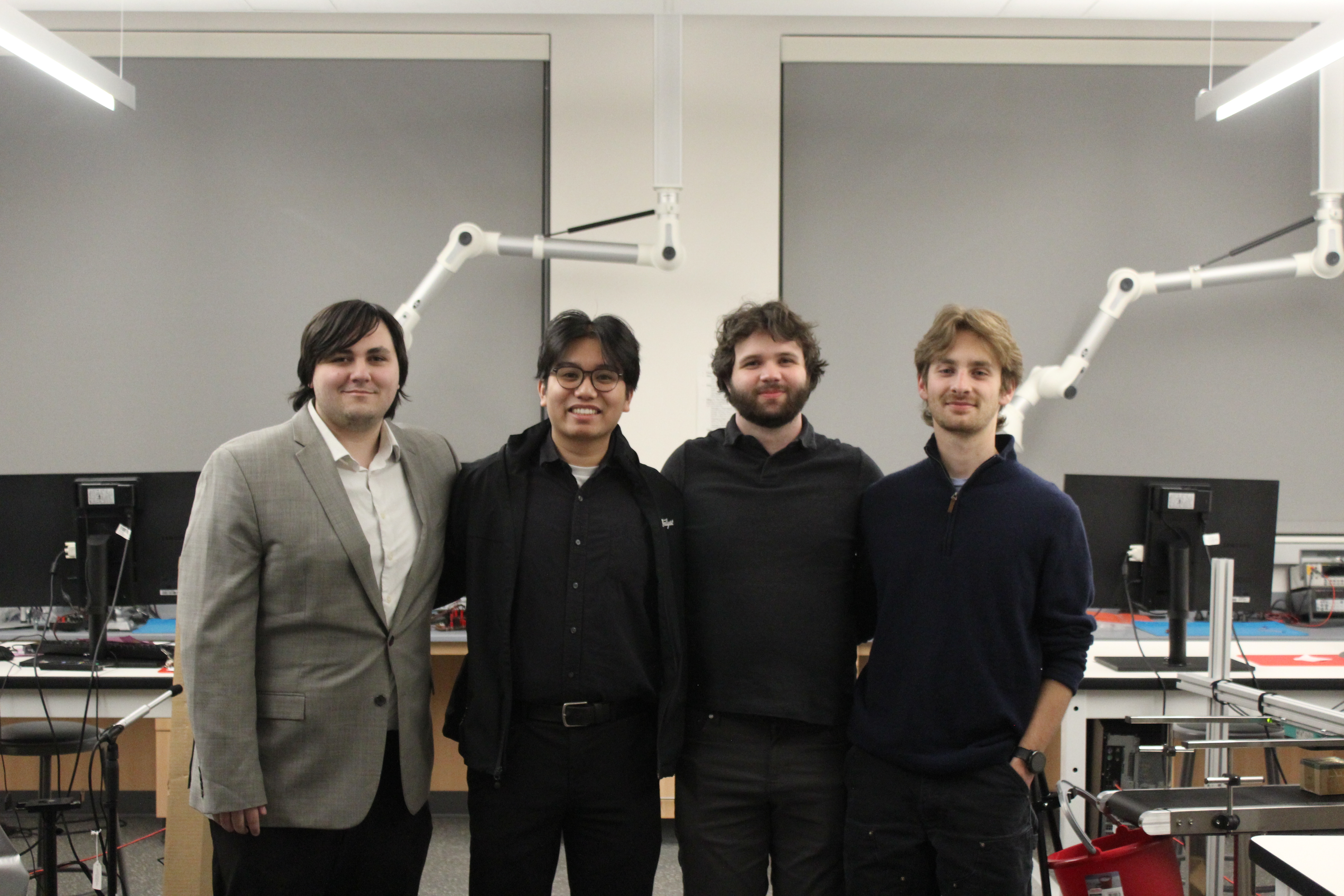
McEwan Bain owned the digital domain on top of this: the I²C bus topology and addressing across the MCU, the GreenPAK configuration interface, the external memory, and the sensor expansion connector. Carlo Cortez owned the analog filter chain after the PGA and the antenna design itself — the matching network on the radio output, the IFA geometry, and the bench tuning we’d do once boards arrive.
Layout: a 4-layer mixed-signal puzzle
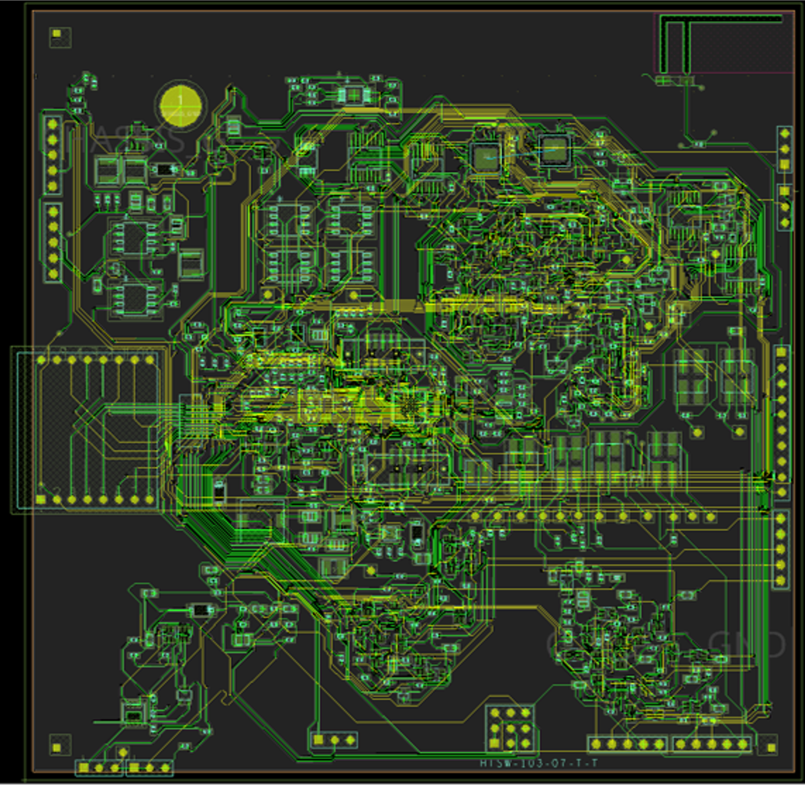
This is the part of the project I owned end-to-end. Schematic capture was a team effort; the layout was mine. With the architecture locked, the constraints I had to satisfy simultaneously were: (1) fan out a 0.4 mm pitch 7×7 BGA, (2) keep digital switching noise off the analog front-end at the tens-of-microvolts signal level, (3) give the radio a clean 50 Ω feed and a usable antenna ground reference, and (4) do it all in 4 layers. Each of those constraints has a clean solution on its own. The interesting work was the layer-stack assignment that satisfied all four at once.
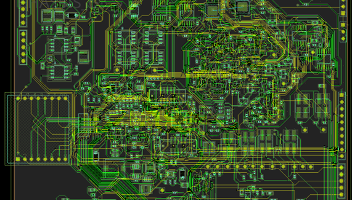
The stackup I ended up with:
- Layer 1 (top): Components, digital signal routing, the MCU and memory, the radio. BGA outer-row escape (dogbone fanout, ~3 mil traces) lives here.
- Layer 2 (inner): Continuous ground, deliberately uninterrupted across the whole board. This is the reference plane for both digital return currents on layer 1 and the 50 Ω microstrip feed to the antenna.
- Layer 3 (inner): Split power planes — separate analog and digital supply pours with a moat between them, and a few signal escapes from the BGA interior dropped down through via-in-pad to be picked up on layer 4. The split is geographic, not just electrical: analog supply pours sit physically under the analog domain on layer 4.
- Layer 4 (bottom): Analog signal routing — the LT1996 input network, the gain-select mux traces, the anti-alias filter, the sensor input connectors. Reference for these traces is the layer-3 analog pour above them.
The reasoning behind the L2/L3 split: a mixed-signal board with a sub-2 µA budget is paranoid about noise coupling. Analog signals at the input of the LT1996 can be tens of microvolts; digital edges from the Apollo3 Blue switching at MHz rates have hundreds of millivolts of spectral content well into the band where the sensor signal lives. Putting digital on layer 1 and analog on layer 4 with a continuous ground plane on layer 2 between them gives the best isolation 4 layers can buy. Any signal trace that crosses from the digital domain to the analog domain does so on layer 1 (where it stays close to layer 2 ground) and lands at the LT1996 input network — it never crosses the analog/digital split on layer 3.
The BGA escape, in detail
A 49-ball 0.4 mm BGA has 24 outer balls (the two outer rings) that can be escaped with conventional dogbone fanout — drop a short stub off the pad, place a via just outside the pad ring, route on an inner layer. That accounts for the rows you can reach from outside. The inner 25 balls (the central 5×5) have no external clearance and require via-in-pad.
I did not want via-in-pad under more balls than necessary, because every via-in-pad is a small reliability and manufacturability cost (epoxy fill, plating-over, thermal asymmetry during reflow). The split I settled on:
- Outer two rows (24 balls): dogbone fanout. Pad → ~3 mil stub → via → fanout trace on layer 1 or layer 4. This is the cheap, well-understood escape.
- Central 3×3 (9 balls): via-in-pad in a diamond pattern. Rather than a straight-grid pattern where every inner-ball via sits directly under its own pad, I staggered them diagonally. The diamond pattern opens diagonal routing channels between adjacent vias that a straight grid blocks entirely.
- The intermediate ring (the 16 balls between the outer rows and the central 3×3): mixed. Where a ball was used and a routing channel was available from the outer ring, dogbone. Where it wasn’t, via-in-pad.
I tried a uniform via-in-pad fill on the inner 25 first. Layer 4 ran out of escape channels — the via stubs descending from layer 1 occupied the same space as the analog traces trying to enter the BGA region from the analog domain. Backing off to the diamond-on-3×3 plan recovered enough channel space to route every inner signal cleanly. The intermediate ring’s per-ball decision was made by walking the layout one ball at a time and asking whether the dogbone escape collided with anything else; where it didn’t, dogbone; where it did, via-in-pad.
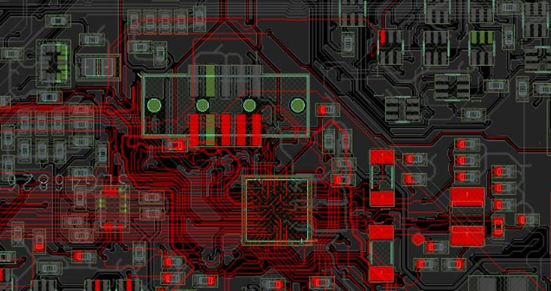
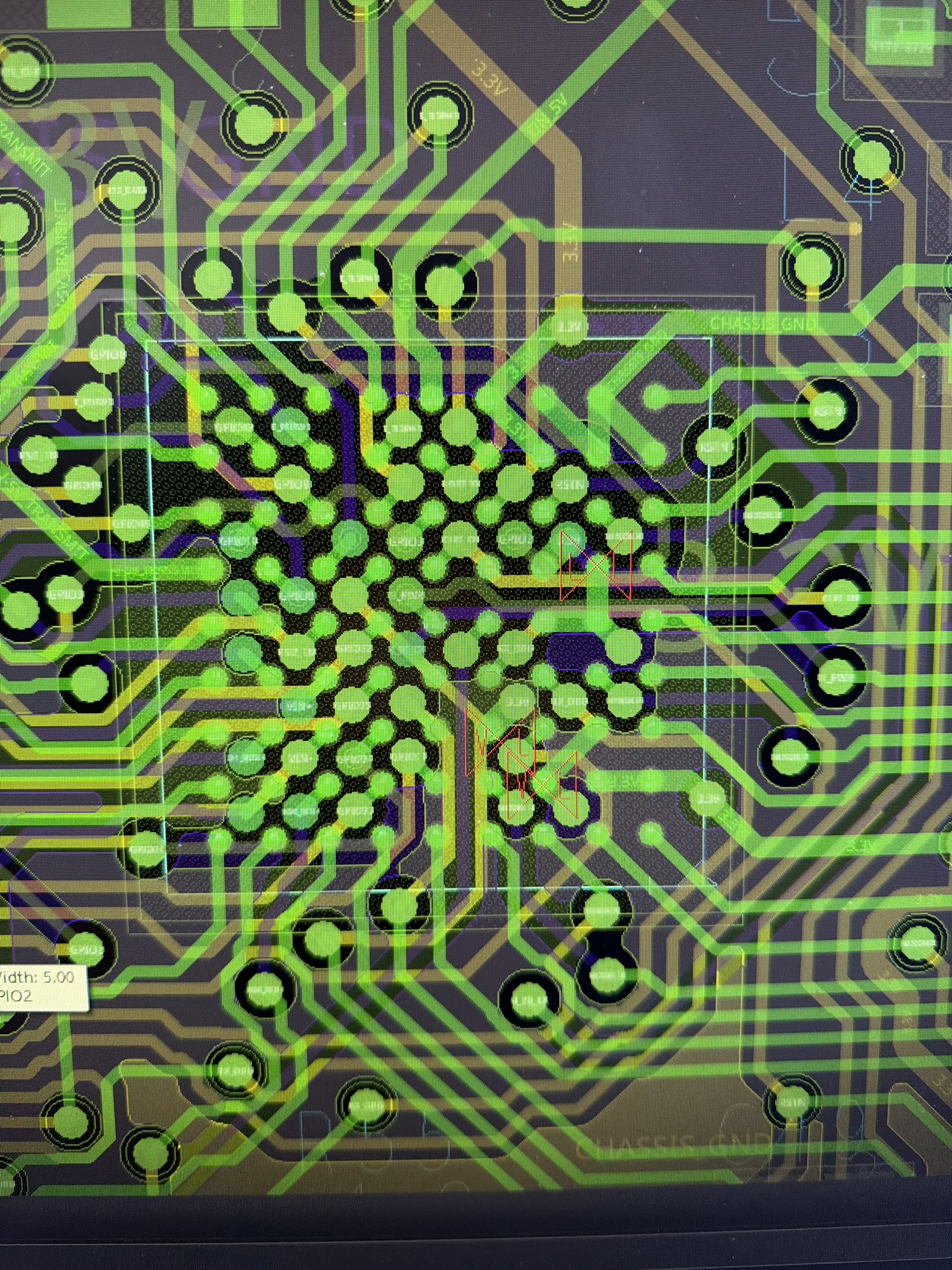
Trace widths in the BGA escape region ran ~3 mil (0.075 mm). That’s the floor for Itron’s PCB partner on a standard 4-layer stackup, and the BGA pitch leaves no choice — anything wider doesn’t fit between adjacent vias. Outside the escape region, traces widen back out (10 mil for signals, 20+ mil for power) where there’s room.
Noise management
Two specific decisions, beyond the layer-stack split itself:
- Star grounding at the LT1996 input. The instrumentation amp’s reference pin and the sensor-side return both tie to a single point on the layer-2 ground plane, not to whatever ground happens to be closest. This kills ground-loop pickup at the input where it matters most.
- Layer-3 split between analog and digital supply pours. The split runs roughly down the middle of the board with no signal traces crossing the split on layer 3. Anything that has to cross does so on layer 1 over the continuous layer-2 ground.
RF: the 2.4 GHz path and the inverted-F antenna
We designed our own 2.4 GHz inverted-F antenna on the PCB rather than using a chip antenna or a module. The reason is mostly that a board this small can’t afford the area cost of a module, and a chip antenna’s matching is sensitive to the exact ground geometry around it in ways that make small-board design a tuning lottery. An IFA is a known shape that’s been characterized to death in the literature; we could lay it out, simulate it, and have a strong prior on what it’d do on hardware.
The routing rules for the RF section:
- 50 Ω single-ended controlled-impedance feed from the radio output through the matching network to the antenna feed point. Microstrip on layer 1, referenced to the continuous layer-2 ground. Trace width set by the stackup’s dielectric and copper thickness — Allegro’s impedance calculator drove the dimension.
- Ground-plane keep-out under the IFA radiating element. No copper on layers 2, 3, or 4 directly beneath the antenna. An IFA radiates because the antenna element and the ground plane act as a resonant structure; pouring ground directly under the radiating element detunes it badly and kills efficiency. The keep-out extends from the antenna feed point out past the antenna tip, with a small margin.
- Component keep-out around the antenna. No nearby copper pours, no via fences, no components within the antenna’s near field on any layer. The corner of the board where the antenna lives is deliberately empty.
- Matching network footprints between the radio and the antenna. A π-network footprint with placeholder 0 Ω links that we’ll populate with real values during bring-up once we sweep S11 on hardware. Designing the matching network purely from simulation on a board this small is asking to be wrong; we built in the ability to tune.
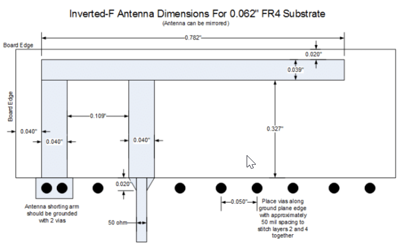
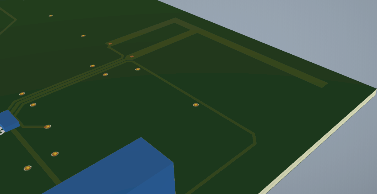
Carlo did the antenna geometry and the matching-network topology. I owned the layout placement — where on the board the antenna sits, the orientation relative to the rest of the design, the keep-out geometry, and the controlled-impedance feed back to the radio.
Power: the math behind sub-2 µA
The quiescent budget is the headline spec, so it’s worth showing where the budget actually goes.
| Subsystem | Sleep current | Note |
|---|---|---|
| Apollo3 Blue deep sleep | ~700 nA | RAM retention + RTC + BOD |
| GreenPAK always-on logic | <50 nA | Wake-on-event watchdog |
| LDO regulator quiescent | ~400 nA | Choice constrained by spec |
| Analog front-end (gated off) | <100 nA | GreenFET reverse leakage |
| Radio (gated off) | <100 nA | GreenFET reverse leakage |
| Sensor input bias | ~200 nA | Pull-down through input network |
| Total | ~1.55 µA | Under the 2 µA target |
The headline number, ~1.55 µA, is the budgeted target. There’s roughly a 25% headroom against the 2 µA spec, which is appropriate — real boards are noisier than computed budgets, and the headroom absorbs surprises like the actual GreenFET off-leakage at temperature, the regulator’s quiescent at our specific load, and any input-bias paths I didn’t anticipate.
What’s done, what’s pending
This is a sponsored capstone with a clear deliverable timeline.
Done:
- Architecture and component selection (Apollo3 Blue, LT1996, GreenPAK + GreenFETs, 2.4 GHz radio + IFA)
- Full schematic capture in OrCAD Capture
- Full PCB layout in OrCAD Allegro 25.1, including BGA fanout (dogbone + diamond via-in-pad split), mixed-signal layer planning, 50 Ω controlled-impedance RF feed, IFA placement and keep-outs
- Design review with Itron’s engineering team
- Bill of materials, manufacturing files, and Gerbers handed off
Pending:
- Manufacturing: board fabrication and assembly through Itron’s PCB partner — currently in their queue
- Bring-up: power-on test, basic functionality checks, JTAG/SWD connection to Apollo3 Blue
- Validation: programmable gain step accuracy, noise floor at each gain setting, deep-sleep current measurement against the sub-2 µA target, wake-on-event latency, S11 sweep on the IFA and matching-network tune
- Sensor characterization: connect representative sensors (current, water flow, temperature) and characterize end-to-end performance
- Final report
When the boards arrive and validation begins, the results section of this case study gets a major update — with real numbers, not budget estimates.
What I learned (so far)
A few takeaways from the design phase that I think will hold up after manufacturing:
Power budgets are architecture decisions. The 2 µA spec wasn’t a number to optimize toward at the end. It dictated the MCU (Apollo3 Blue), the gain stage topology (LT1996 + mux instead of digital PGA), the wake-on-event approach (GreenPAK instead of MCU-pin polling), and the load-switching strategy (GreenFETs gating everything that can be gated). A board designed without that budget in mind would have ended up at 10–20 µA almost regardless of what you optimized later. Tight power constraints are best treated as a top-of-tree decision, not a finishing pass.
Layout is where mixed-signal design either works or doesn’t. A schematic that looks clean can produce a board that doesn’t meet noise spec because of where a return current ended up routing, or because a digital trace skirted the analog domain on the wrong layer. The work that happened in Allegro — layer assignment, BGA escape pattern, IFA keep-out, the L3 power split, the star ground at the LT1996 — wasn’t decoration on a finished schematic; it was a second design pass at the same problem. I spent more time on layout than on schematic capture, and I’d do that ratio again.
Sponsored capstone is a different kind of engineering than coursework. Itron isn’t grading a homework set; they’re going to manufacture this board. That changes the bar in specific ways — design reviews are real reviews, the BOM has to source against parts the sponsor’s supply chain actually carries, the manufacturing files have to match the sponsor’s PCB partner’s submission requirements, the timeline is constrained by their queue, not yours. Some of this is “industry vs. academia” in a way that’s been written about elsewhere; the part that surprised me is how much project management was actual engineering work. Choosing what to lock down and when, choosing whose work blocks whose, choosing what to push back to the sponsor and what to absorb — these are engineering decisions, made with the same kind of tradeoff reasoning as the gain-stage choice.
Team capstone work is harder than it looks from outside. Four people, four areas of ownership (architecture/PM/layout, power/BGA, digital/I²C, filter/antenna), one shared schematic and one shared layout. The thing I’d do differently next time: designate a single layout owner from day one (which ended up being me, but informally) with explicit authority to push back on schematic-side changes once placement was committed. Late schematic edits that look trivial — a pin swap, an added decoupling cap, a connector moved by 2 mm — can blow up a BGA escape that took two days to settle. Making that authority explicit early would have saved a few rounds of rework.
When the boards come back from Itron’s queue and validation starts, this case study gets a results section. Until then, this is a design case study, not a results one — and I’d rather be honest about that distinction than gesture at numbers that don’t exist yet.
If you’re working on similar problems — universal analog front-ends, sub-µA power budgets, GreenPAK-as-glue-logic architectures, or HDI BGA escapes on tight 4-layer stackups — email me. There’s not a lot of public writing on this part of the field.